10+ kicad block diagram
Copy path Copy permalink. The KiCad project is proud to announce the latest series 5 stable release.

My First Pcb Layout Projects Kicad Info Forums
A list of all of the fixed bugs since the 519 release can be found on the KiCad 5110 milestone page.

. This release contains several critical bug fixes so. Creating schematics involves picking components from the Kicad library and. The default soldermask clearance is 01mm per side in Eagle.
All installer binaries will have a code signed digital signature attached. Voltastream0-kicad Block_Diagramsch Go to file Go to file T. Windows will automatically verify the signature is valid however you may want to ensure it.
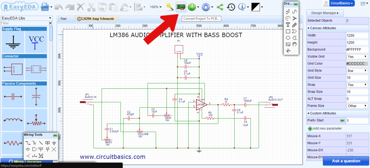
Go to line L. Click New under templates or categories click General and then double-click Block Diagram. Cannot retrieve contributors at this time.
The 5110 stable version contains critical bug fixes and other minor improvements since the previous release. 7161 lines 7161 sloc 672 KB. KiCad expects to nd the schematic les of hierarchical.
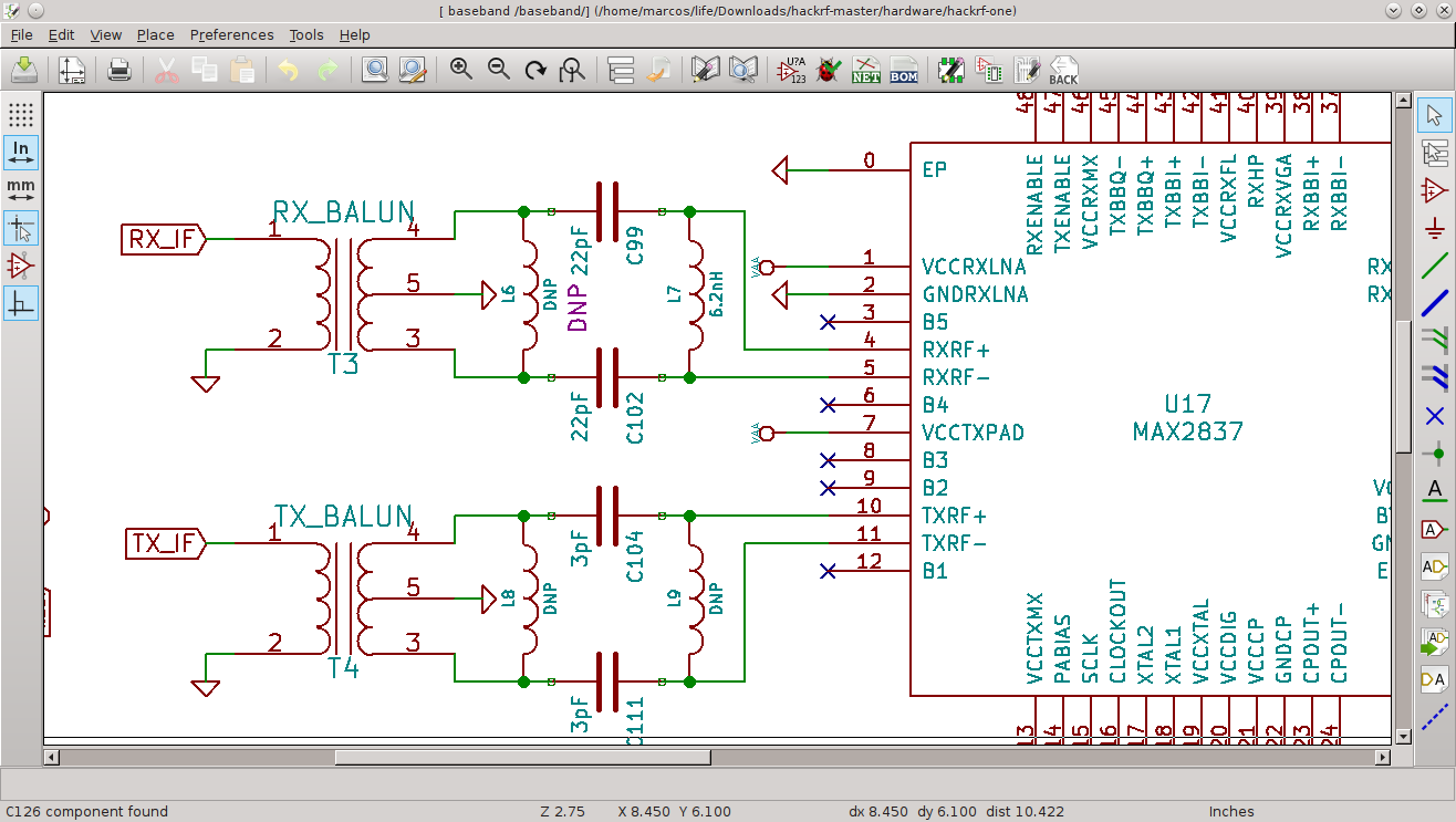
STREAM hardware STREAM v2 v2r1 KiCAD Board block diagramsch Go to file Go to file T. We can now proceed to start placing components on the canvas to draw our schematics. Block you should make ALL connections to the outside as hierarchical pins.
Cannot retrieve contributors at this time. Go to line L. Copy path Copy permalink.
From the Blocks and Blocks Raised stencils. Click the File tab. 5 The insertion of buildingblocks into a schematic 10.
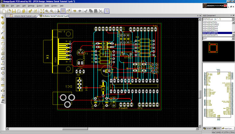
Unfortunately I dont believe. In KiCads Pcbnew open the ZOPT220x Breakout and click on Dimensions - Pads Mask Clearance. Create a block diagram.
Quick tutorial on how to create an exploded assembly diagram from a KiCad PCB using Fusion 360s Animation and Drawing tools.

Kicad Wikiwand
My First Pcb Layout Projects Kicad Info Forums

My First Pcb Layout Projects Kicad Info Forums

Schematic Review Pid Controller Anything Look Wrong R Printedcircuitboard

Noob Questions Hidden Pin Mystery Erc And Net Id Schematic Kicad Info Forums
סבא מימי מוחלט Schematic Diagram To Pcb Layout Software Kagitakademisi Com

Kicad Pcb Tml
סבא מימי מוחלט Schematic Diagram To Pcb Layout Software Kagitakademisi Com

Schematic Capture Wikiwand

Kicad Wikiwand

Trying To Make An Arduino Shield Need Help With Layout Layout Kicad Info Forums
סבא מימי מוחלט Schematic Diagram To Pcb Layout Software Kagitakademisi Com

Noob Questions Hidden Pin Mystery Erc And Net Id Schematic Kicad Info Forums

My First Pcb Layout Projects Kicad Info Forums

Noob Questions Hidden Pin Mystery Erc And Net Id Schematic Kicad Info Forums

Tutorials For Kicad A Free Open Source Schematic And Pcb Layout Editor Curious Inventor Circuit Board Design Tutorial Circuit Board

Need Help Using Replicate Layout Plugin Layout Kicad Info Forums